| |||||||||||||||||||||||||||||||||||||||||||||||||||
|
 |
||||||||||||||||||||||||||||||||||||||||||||||||||
Contact : 022-21596863 Email Id : fegsemlab@iitb.ac.in | |||||||||||||||||||||||||||||||||||||||||||||||||||
1. A requisition letter addressed to Head, SAIF along with a printout of electronic fund transfer (NEFT) proof should be sent by post or
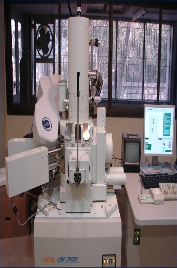
submitted in person to SAIF office, IIT Bombay, Powai, Mumbai-400076. 2. If you are not supposed to be present during the measurements, please mention as many details as possible, such as: a. Expected features you are looking for (send a representative picture if available). b. Images up to what magnification factor you want. c. Nature of your sample, for example, whether it is conducting or non-conducting. d. If it needs to be dispersed in any solvent (for powdered samples). If required, please attach a separate sheet. 3. Once we receive the requisition letter and advance payment, you will receive tentative date of appointment. 4. The user will be informed about their date and time of slot by e-mail. 5. The sample should be dry and should withstand high vacuum ( ~ 10 -5 Pa). Wet biological sample can’t be done in FEG-SEM 6. The sample size should be less than 12.5 mm x 12.5 mm x 10 mm (height) and the side opposite the side of interest, should be flat (to enable sample mounting). The smaller the sample height the better. 7. The user is welcome to be present in the laboratory during analysis. 8. Before proceeding further, please review How to Use Facility and Payment Procedure for more information. |
|||||||||||||||||||||||||||||||||||||||||||||||||||
|
|
|||||||||||||||||||||||||||||||||||||||||||||||||||
| |||||||||||||||||||||||||||||||||||||||||||||||||||