|
|||||||||||||||||||||||||||||||||||||||||||||||||||||||||||||||||||||||||
|
 |
||||||||||||||||||||||||||||||||||||||||||||||||||||||||||||||||||||||||
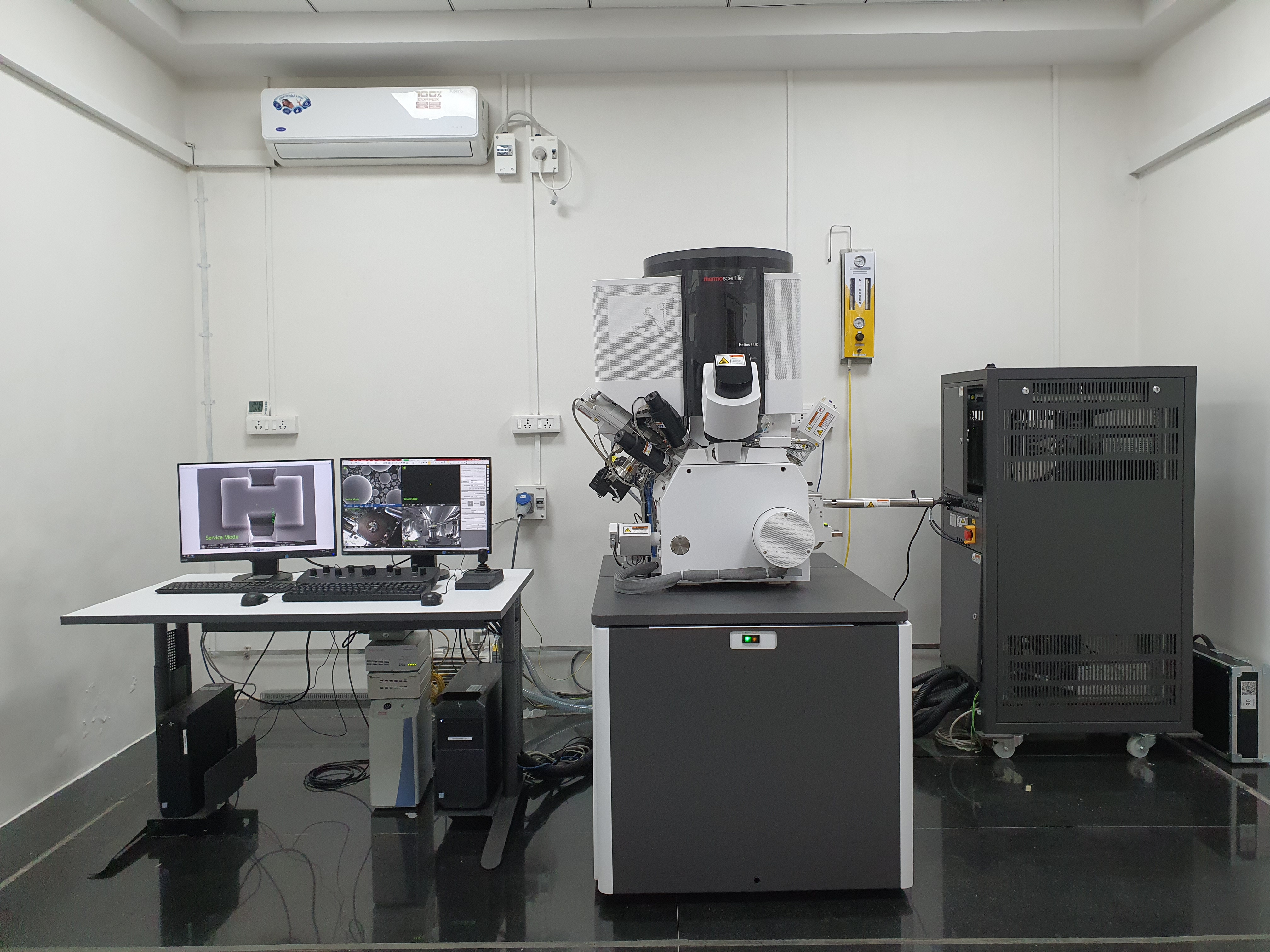
The Helios 5 UC model combines the Scanning Electron Beam (SEM) and the Focused Ion
Beam (FIB) in order to achieve analysis at |
|||||||||||||||||||||||||||||||||||||||||||||||||||||||||||||||||||||||||
1. Energy Dispersive Spectroscopy (EDS): Thermo Fischer Scientific UltraDry EDS Detector ; 100mm² active detection area ; Norvar Window with proprietary evacuated tube design for detection sensitivity to Be ; 129eV resolution at Mn K-alpha 2. Retractable STEM Detector: , For Bright Field/Dark Field/High Angle Annular Dark Field imaging of thin samples. 3. GIS for deposition and etch: Ion and e-beam assisted deposition sources includes Platinum, Carbon and Insulator (SiO2). 4. Micromanipulator: For easy lift-off of lamella. |
|||||||||||||||||||||||||||||||||||||||||||||||||||||||||||||||||||||||||
1. TEM lamella preparation 2. Site specific Cross sectional imaging , 3D Slice and View 3. Precision machining for micro tools 4. HR imaging, Low kV HR imaging , SEM/STEM imaging , Ion beam imaging 5. Nano-fabrication and Nano-patterning |
Contact : 022-21596861 Email Id : fibsem@iitb.ac.in |
||||||||||||||||||||||||||||||||||||||||||||||||||||||||||||||||||||||||
|
|
|||||||||||||||||||||||||||||||||||||||||||||||||||||||||||||||||||||||||
A) External Users (other than IIB users) 1. External Users (other than IIB users) would need to do online registration through the I-STEM portal. To proceed with the registration, users are requested to fill out the MSDS form and a cover letter. The required formats are available for download on the I-STEM portal. Please ensure that all sections of both documents are completed, including the necessary signatures and official stamp. Kindly upload the duly filled MSDS form and cover letter on the I-STEM portal. Please find attached a PDF guide outlining the registration process through I-STEM for your convenience ( ISTEM Registration Guidelines for external users ). Before registering the samples for this facility, users are requested to contact the FIB-SEM lab (Phone No. : 022-21596861; Email Id: fibsem@iitb.ac.in) to discuss about the sample analysis. You may decide the charges to be paid after mutually understanding the analysis requirements. 2. After the online registration is completed, the appointment will be scheduled as per the queue. 3. The users will be informed about their date and time of slot by e-mail. 4. We prefer that you or your representative, who knows / understands the sample / material, should be present on the day of appointment. 5. After registration, samples can be sent by post or submitted in person to SAIF/CRNTS office, IIT Bombay, Powai, Mumbai-400076. B) Internal Users (IIB users) 1. Internal Users (IIB users) would need to do online registration through the DRONA portal. When user clicks ‘DOWNLOAD button’, this webpage will open. Internal Users are requested to fill out sample request form / MSDS form inorder to understand the sample analysis requirements (MSDS Form for internal users ). All the other registration steps need to be done through the DRONA portal. 2. We prefer that you or your representative, who knows / understands the sample / material, should be present on the day of appointment. |
|||||||||||||||||||||||||||||||||||||||||||||||||||||||||||||||||||||||||
|
|
|||||||||||||||||||||||||||||||||||||||||||||||||||||||||||||||||||||||||
|
|||||||||||||||||||||||||||||||||||||||||||||||||||||||||||||||||||||||||