|
||||||||||||||||||||||||||||||||
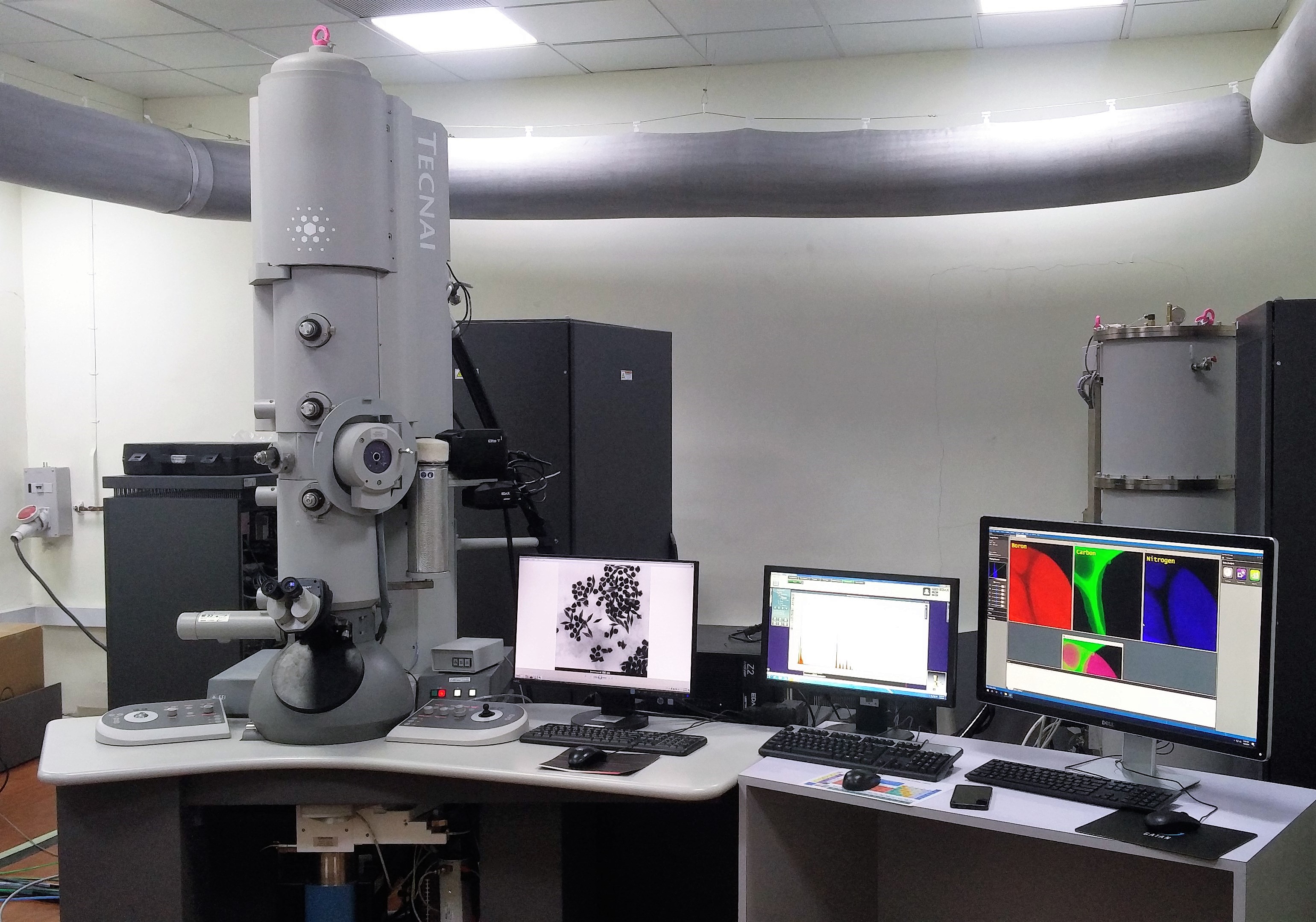
Energy Dispersive Spectroscopy (EDS): EDAX Octane ELITE T70 STEM: Bright Field/Dark Field/High Angle Annular Dark Field detectors Electron Energy Loss Spectroscopy (EELS): Model 965 GIF Quantum A post column Energy Filter with Dodecapole-based optics for very low image distortions for EFTEM imaging, mapping, and spectroscopy and optimized STEM-EELS mode, operating with a separate computer running on 64 bit PC hardware and Win 7 OS environment with latest version of GMS s/w suit for capture and processing. |
Contact :
022-21596864
Email Id : fegtem300@iitb.ac.in |
|||||||||||||||||||||||||||||||
External Users (other than IIT Bombay): 1. A requisition letter addressed to Head, SAIF along with a printout of electronic fund transfer (NEFT) proof should be sent by post or submitted in person to SAIF office, IIT Bombay, Powai, Mumbai-400076. 2. Once your requisition letter along with the payment proof is received by the SAIF office, your appointment will be scheduled as per the queue. 3. The user will be informed about the appointment date and time by e-mail. 4. The sample can be loaded on a carbon coated copper grid or can be made in disc form, 3mm diameter, with a thinned (electron transparency) central area. 5. It is desirable that the user is present in the TEM lab at the time of the appointment for better utilization of the facility. 6. Before proceeding further, please review How to Use Facility and Payment Procedure for more information. Internal (IIT Bombay) Users: 1. The user should register online. 2. An appointment will be given as per the queue and the user will be informed by an email. 3. The new user is requested to contact TEM Lab before registration. |
||||||||||||||||||||||||||||||||
|
||||||||||||||||||||||||||||||||